Package Design
In response to the difficulty of maintaining Moore's law, new high-density advanced packaging technologies have been developed. These include fan-out wafer-level packaging, chip-on-wafer-on-substrate, and wafer-on-wafer technology. These various technologies help pack more computational power into a smaller space in the most efficient ways possible.
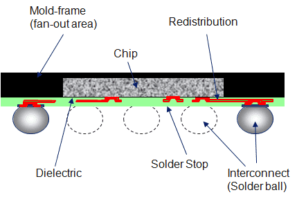
Fan-out wafer-level packaging (FOWLP), in contrast to normal wafer-level packaging (WLP), offers a smaller package footprint with improved electrical and thermal performance. With FOWLP, there can be more contacts on a die without increasing its size. The wafer is diced first, just like in normal WLP, but then each die is carefully re-positioned on a carrier wafer or panel, leaving space for fan-out, which leads to the ability to form more complex circuits. This results in having a package which is much larger than the die size itself, as opposed to normal wafer-level packaging.